ELECTRICAL ENGINEERING · TEXAS TECH UNIVERSITY
Electrical engineering student focused on RF circuit design
My portfolio includes a 40 MHz Hartley oscillator, a software-defined FM radio, and an industrial communication system evaluation from my internship at Diamondback Energy, along with a 137 MHz weather satellite receiver in progress at bottom of site.

B.S. EE, December 2026
M.S. EE, May 2028
PROJECT SHORTCUT
1:
Software-Defined FM Radio
ECE 3334 / Signal Processing Chain

Fig 1.1: Python processing chain - RTL-SDR capture through audio conditioning
Project Summary
DSP Chain Technical Details
Three-person project tasked with building a portable FM receiver where I owned the signal-processing chain written in Python and running on a Raspberry Pi 5. The unit receives and plays local FM stations on battery power through a touchscreen interface, utilizing an RTL-SDR V4 and a custom 50-ohm filter.
Video Demonstration: https://youtu.be/yy4hhP87rsU?si=1iEK0dQr7ZUYm6y9
- Digital oscillator and mixer shifting selected stations to baseband.
- 41-tap FIR low-pass filter and decimation for optimized processing.
- FM demodulation via phase discriminator using current and conjugate samples.
- Audio conditioning including de-emphasis, DC removal, and resampling.


Fig 1.2: Front view of SDR FM Receiver
Fig 1.3: MATLAB program illustrating IQ phasor and corresponding in-phase waveform showing a varying rate of change, resulting in instantaneous frequency deviation
2:
Industrial Communication System Evaluation
Intern project
Project Summary

Evaluated two control system architectures, the Instrumentation Junction Box (IJB) and Remote Input/Output System (RIO) for oil and gas production facilities and recommended remote I/O as the new standard, cutting installed cost by roughly 22% per facility while adding Device Level Ring redundancy to eliminate its single point of failure.
WHAT I DID
-
Drew and field-verified bid-level drawings for both architectures
-
Conducted a cost comparison which showed remote I/O about 22% cost reduction per facility
-
Simulated fault scenarios and reviewed three years of downtime data
-
Implemented a failover network for architecture, Device Level Ring, and verified failover in the lab
-
Wrote a configuration guide for future builds
Fig 2.1: Block Diagram of Instrumentation Junction Box Architecture


Fig 2.2: Block Diagram of Remote Input/Output Architecture
Fig 2.3: Block Diagram of Device Level Ring Topology
3:
40 MHz Hartley Oscillator
Individual project

CIRCUIT SCHEMATIC & PARAMETERS
- Transistor Type: 2N3904 NPN Transistor
- Supply Voltage: 12 V DC Laboratory Rail
- Tank Inductor: 384 nH (L1) & 96 nH (L2) Tapped Sections
- Tank Capacitor: 33 pF
- Feedback Topology: Inductive Tapped Feedback Network
Fig 3.1: 40 MHz Hartley Oscillator Schematic
Measured Bench Performance Diagnostics
Measured Frequency: 40.1 MHz vs 40.0 MHz target frequency (representing a 0.25% tuning variance). Scope shows harmonic distortion.
Signal Amplitude: 1.79 Vpp sinusoidal output under standard active load.
Tuning Methodology: First physical build resonated layout at 32 MHz. Precise adjustment of the coil tap location and optimizing the L1:L2 feedback ratio successfully brought the circuit near frequency.


Fig 3.2: Copper clad build with hand-wound air-core inductors
Fig 3.3: Measured output of oscillator build
Work in Progress

137 MHz Satellite Receiver (RF Front End)
Three-person superheterodyne receiver for a 137 MHz weather satellite downlink, built from discrete components. I own the RF front end: a 50-ohm preselector bandpass filter, mixer, and LNA. The project will be validated with a signal generator in place of a live satellite downlink, but it is designed as a real weather satellite receiver.
DESIGNED AND VERIFIED: FILTER AND MIXER
Weather Satellite Receiver Bandpass Filter Design
-
Designed a 6 MHz preselector 4th order Chebyshev bandpass filter centered at 137.5 MHz between 50-ohm terminations
-
Direct-Coupled Shunt Capacitor topology
-
Utilized combination of series and inductor calculations to match capacitor values in schematic
-
Passes 133.8 MHz to 139.79 MHz
-
Insertion loss of 8.4dB - 8.6 dB
-
5.9MHz 3 dB BW
-
Video Demonstration: https://youtu.be/3hKbTohQf2U?si=1VhUCejccCE8FIEi

Fig 4.1: Preselector 6 MHz bandpass filter design


Fig 4.2: Copper clad build of bandpass schematic
Fig 4.3: Vector Network Analyzer measurement displaying 6 MHz bandpass filter response
Fig 4.3: Vector Network Analyzer measurement displaying 6 MHz bandpass filter response
SLIGHT IMPROVEMENT OF BANDPASS FILTER
-
VNA measurements after inductor tuning showed insertion loss dropping from 8.5 dB to 4.35 dB at 137.5 MHz
-
3 dB bandwidth reduced from 5.9 MHz to 5.7MHz
-
Found that insertion loss could be lowered further to 2 dB, but only by widening the bandwidth to 8 MHz
-
Used 1% Tolerance capacitors


Fig 4.4: Rebuilt Bandpass Filter
Fig 4.5: Vector Network Analyzer measurement displaying optimized filter response
DOUBLE BALANCED DIODE RING MiXER DESIGN
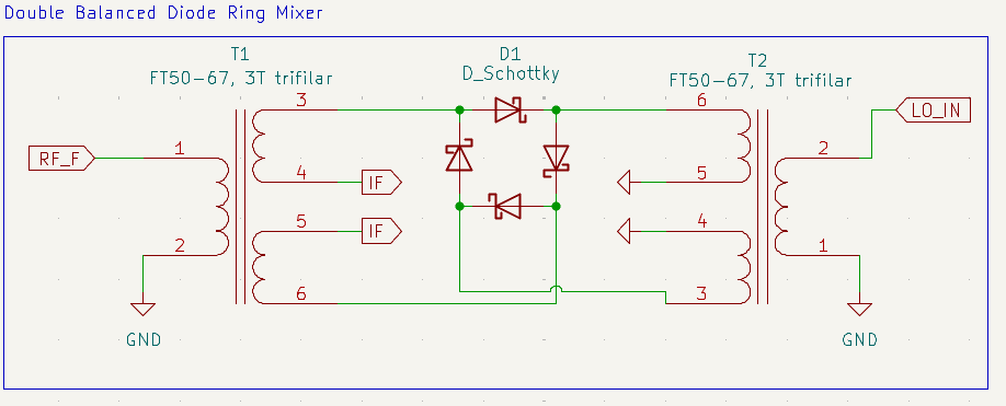
-
Balun transformers wound on 0.5" OD 67-material ferrite toroids, selected for low loss and low permeability suited for 137 MHz
-
BAT81S Schottky diodes selected for low forward voltage and low junction capacitance (1.8 pF), reducing required LO drive
-
~300nH inductance on each toroid
-
Target of at least 20 dB LO-RF, LO-IF, and RF-IF isolation
Fig 4.6: Double Balanced Diode Ring Mixer Design
DOUBLE BALANCED DIODE RING MiXER BUILD AND RESPONSE
-
6.85 dB conversion loss (Expected 7dB Loss in design)
-
30dB Isolation for RF-IF and LO-IF ports
-
-20dBm RF input at 137.5 MHz
-
7 dBm LO Input at 126.8 MHz


Fig 4.7: Double Balanced Diode Ring Mixer copper build
Fig 4.8: IF frequency reading illustrating 6.85 dB conversion loss with a -20 dBm RF input


Fig 4.9: LO frequency reading illustrating 30 dB LO-IF isolation with a -20 dBm RF input
Fig 4.10: RF frequency reading illustrating 30 dB RF-IF isolation with a -20 dBm RF input
PCB DESIGN

-
To be built and tested
-
MAR-1SM gain stage as the LNA ahead of the preselector
-
1.26 mm grounded coplanar waveguide (0.2 mm gap) on 1.6 mm FR-4 for 50 Ω RF, LO and IF lines
-
Length-matched mixer ring traces (25.1 to 27.1 mm) to keep the balun phase balanced and preserve port-to-port isolation
-
Isolated the RF, LO and IF paths with via fencing, solid top and bottom ground pours, and connectors on separate board edges


Fig 4.11: Full RF Front End Schematic
Fig 4.12: PCB design and layout
Fig 4.12: 3D View of PCB Layout